
Blog
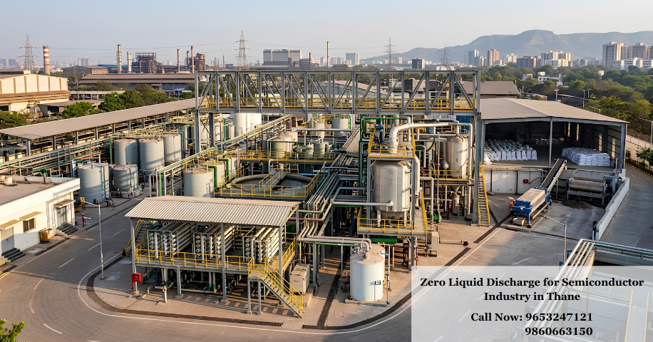
Zero Liquid Discharge for Semiconductor Industry in Thane



 Enquire Now
Zero Liquid Discharge for Semiconductor Industry in Thane | Aquacaresee
Call Now: 9653247121
Website: https://aquacaresee.com
About Aquacaresee Pvt. Ltd.
What Is Zero Liquid Discharge for the Semiconductor Industry?
Zero Liquid Discharge, commonly called ZLD, is a wastewater treatment strategy in which treated wastewater is recovered for reuse and the remaining concentrated waste is further processed so that no routine liquid effluent is discharged from the treatment system.
In semiconductor manufacturing, wastewater streams can originate from several operations, including wafer rinsing, etching, cleaning, polishing, cutting, chemical processing, equipment cleaning, and water purification systems.
The exact wastewater composition varies from facility to facility. Depending on the manufacturing process, wastewater may contain suspended solids, dissolved salts, fluoride, metals, changes in pH, organic compounds, and other process-specific contaminants.
Therefore, a semiconductor ZLD plant should not be selected simply by capacity. It should be engineered after understanding the actual wastewater profile.
The U.S. EPA identifies semiconductor wastewater sources such as etching, cleaning, degreasing, cutting and grinding, with pollutants including fluoride, arsenic and organic compounds.
How Does a Semiconductor ZLD System Work?
A typical ZLD approach may combine several treatment technologies depending on the wastewater characteristics.
A simplified treatment sequence can include:
Wastewater Collection → Segregation → Pretreatment → Clarification/Filtration → Membrane Treatment → RO → Evaporation → Concentration/Drying → Water Recovery → Reuse
Not every semiconductor facility will require exactly the same configuration. Process design should be based on laboratory analysis, wastewater characterization, recovery targets, operating conditions, and the intended reuse application.
Why Semiconductor Manufacturers in Thane Need Advanced Wastewater Treatment
Semiconductor manufacturing is a water-intensive industrial activity because high-purity water is required for numerous production processes.
The water used in semiconductor facilities is not simply ordinary process water. Ultrapure water and deionized water can be required for manufacturing and rinsing applications. EPA documentation notes that semiconductor facilities use treated water for applications such as wafer rinsing, acid-related processes, equipment cleaning, and cutting and grinding operations.
For companies operating in Thane and the wider Maharashtra industrial ecosystem, water reuse can also become an important part of long-term environmental management.
Semiconductor Wastewater Can Be Complex
Unlike wastewater from a single conventional process, semiconductor wastewater may contain different streams generated by different manufacturing activities.
For example, wastewater can come from:
- Wafer rinsing
- Etching operations
- Chemical cleaning
- Surface preparation
- Polishing
- Cutting and grinding
- Equipment cleaning
- Scrubber systems
- RO reject
- UPW system reject
- Process cooling applications
- Facility and utility operations
EPA studies have documented semiconductor wastewater streams associated with ultrapure-water reject, rinsing after etching, photolithography, polishing and other manufacturing operations.
Because these streams may have different characteristics, wastewater segregation and characterization can be important parts of a successful treatment strategy.
Key Components of a ZLD System for Semiconductor Manufacturing
A ZLD system is an integrated treatment process designed to recover water and minimize liquid discharge. Depending on wastewater characteristics, Aquacaresee can consider the following components:
1. Wastewater Collection & Segregation
Different streams such as acidic, alkaline, fluoride, high-TDS and metal-bearing wastewater may require separate collection and treatment.
2. Pretreatment
Processes may include equalization, pH adjustment, neutralization, coagulation, flocculation, clarification and filtration to prepare water for advanced treatment.
3. Ultrafiltration (UF)
UF helps remove suspended and colloidal matter and can provide effective pretreatment before RO.
4. Reverse Osmosis (RO)
RO recovers treated water as permeate while concentrating dissolved salts and contaminants in the reject stream.
5. Evaporation
MEE systems can further concentrate RO reject while recovering water as condensate.
Benefits of Zero Liquid Discharge for Semiconductor Industry in Thane
Choosing Zero Liquid Discharge for Semiconductor Industry in Thane can offer several benefits when properly designed for the facility’s wastewater characteristics.
1. Higher Water Recovery
Why Choose Aquacaresee for ZLD in Thane?
Choosing the right ZLD provider is important because semiconductor wastewater can vary based on manufacturing processes. Aquacaresee Pvt. Ltd., established in 2006, provides customized water and wastewater treatment solutions.
1. Experienced Since 2006
Aquacaresee has extensive experience in water and wastewater treatment, offering ZLD, ETP, WWTP, RO, UF and related solutions.
2. Customized Engineering Approach
Each ZLD system can be designed based on wastewater flow, pH, TDS, COD, fluoride, metals, suspended solids, recovery targets and reuse requirements.
3. Complete Project Support
Aquacaresee supports projects from site assessment and wastewater analysis to design, manufacturing, installation, commissioning, AMC and O&M, providing an end-to-end approach to ZLD implementation.
Customized ZLD Solutions for Different Semiconductor Applications
Semiconductor facilities generate different wastewater streams depending on their manufacturing processes. Therefore, ZLD systems should be customized according to actual wastewater characteristics.
Wafer Manufacturing
Cutting, grinding, polishing, cleaning and rinsing can generate wastewater containing solids and dissolved contaminants requiring suitable pretreatment.
Etching and Cleaning
These processes may produce acidic, alkaline or chemical wastewater, making proper segregation and treatment important.
UPW and RO Reject
UPW and RO systems can generate concentrated reject streams that may be evaluated for recovery and reuse within the facility.
Utility Wastewater
Cooling systems, scrubbers and other utilities can produce additional wastewater streams that may be treated separately or integrated into the overall ZLD system.
Experience • Expertise • Authoritativeness • Trustworthiness (E-E-A-T)
Experience
Aquacaresee has been operating in the water and wastewater treatment field since 2006, providing treatment systems and related services.
Expertise
The company works across multiple treatment technologies, including ZLD, ETP, WWTP, RO, UF, STP and other water treatment systems.
Authoritativeness
Aquacaresee’s website identifies a broad industrial portfolio and reports experience across more than 25 industrial segments, along with engineers and associates and water–recycling projects.
Trustworthiness
Frequently Asked Questions (FAQs)
Q1. What is Zero Liquid Discharge in semiconductor manufacturing?
Ans: Zero Liquid Discharge is a wastewater treatment approach designed to recover and reuse treated water while concentrating the remaining dissolved contaminants into a solid or manageable residue, minimizing or eliminating routine liquid discharge.
Q2. Why is ZLD important for semiconductor industries?
Ans: Semiconductor manufacturing uses significant quantities of high-quality water and can generate wastewater from rinsing, etching, cleaning, polishing, UPW systems and other processes. ZLD can help increase water recovery, reduce liquid discharge and support water-reuse objectives.
Q3. Can ZLD treat semiconductor wastewater?
Ans: Yes, ZLD can be engineered for semiconductor wastewater, but the treatment configuration should be based on wastewater characterization. Different streams may require segregation and specific pretreatment before membrane and evaporation processes.
Q4. What technologies are used in semiconductor ZLD plants?
Ans: Depending on wastewater characteristics, a ZLD system may include equalization, pH correction, chemical precipitation, clarification, filtration, UF, RO, MEE, ATFD and other specialized treatment technologies.
Q5. Can recovered ZLD water be reused in semiconductor manufacturing?
Ans: Potentially, yes. However, the required quality depends on the reuse application. Water intended for high-purity semiconductor processes may require additional purification and polishing before reuse. Semiconductor water-reuse systems are generally designed according to site-specific water-quality requirements.
Contact Aquacaresee Pvt Ltd
- Phone:+ 91 – 96532 47121 / + 91 – 98606 63150
- Email: marketing@aquacaresee.com
- Website: www.aquacaresee.com
- Add: 8th floor office No.810, KAMDHENU 23 WEST, TTC Industrial Area, MIDC Industrial Area, Pawne, Navi Mumbai, Maharashtra 400705, Navi Mumbai, Maharashtra 400705.
- Add: Office No. 204, Aquacaresee Pvt. Ltd.; 205; and 206, Old Mumbai-Pune Hwy, opp. Hotel Silver Seven, Akurdi Gaothan, Vivek Nagar, Akurdi, Pimpri-Chinchwad, Pune, Maharashtra 411035.
- Add: Hanuman Vatika, F/1 – 56-A/3, I, opposite Golden Dags Resorts, near 200 Feet Bypass Road, Hanuman Vatika-1, Heerapura, Heerawala, Jaipur, Rajasthan 302024.
Conclusion
A properly engineered Zero Liquid Discharge for Semiconductor Industry in Thane solution can integrate pretreatment, membrane filtration, reverse osmosis, evaporation and final concentration technologies to recover water and manage concentrated waste.
Call Now: 9653247121
“Don’t forget to share this post!”